Back to homepage
PIC microcontrollers
Introduction
PIC microcontrollers are a well known series of microcontrollers from
Microchip.
Their good sides are low price, and a whole lot of stuff included on board (depending on model):
Flash, Eeprom, USART, timers, counters, A/D converters, PWM, etc.
Chip programmers are reasonably priced.

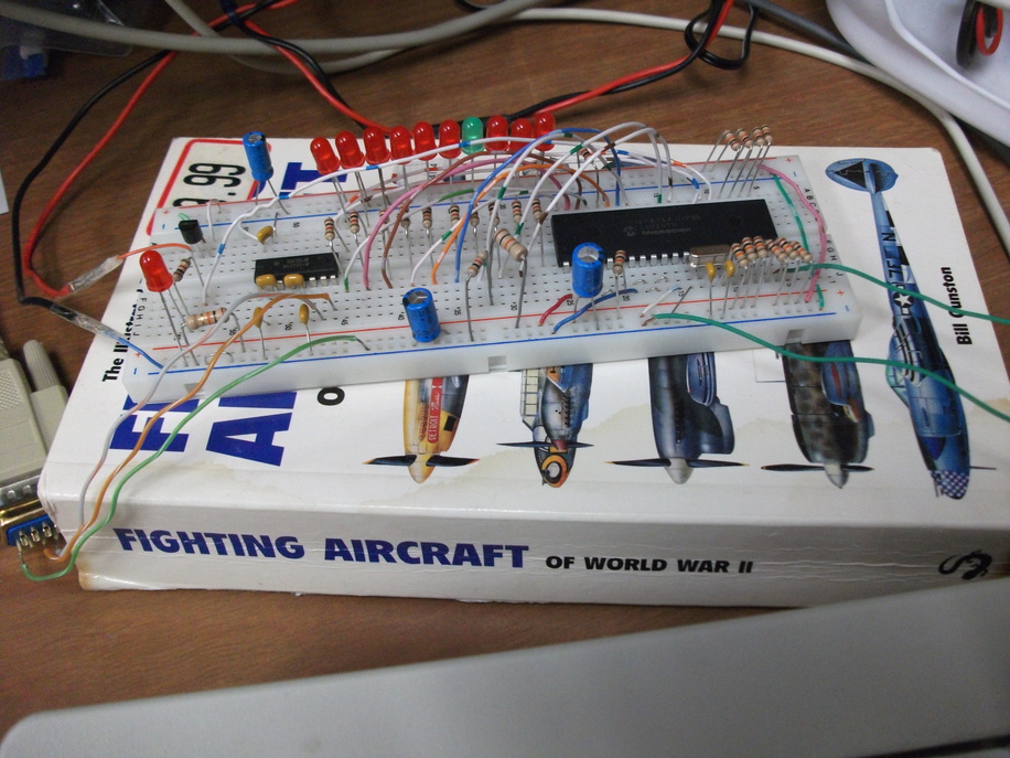
Test setup. Serial port wires connect to MAX232 chip. PIC 16F874A microcontroller is on the
right side of the protoboard.
Serial port was used to send read/write and test commands to PIC.
LEDs are used to indicate status of some microcontroller pins. PGM pin (36, PORTB 3)
should be grounded, in picture it is shown incorrectly connected to +5 V.
ICSP is not used :)

PIC bad sides are incredible variety of partially or fully incompatible models:
for example, PIC 16F874 and 16F874A have different ways for writing to Flash memory,
so your old code for Flash writing for 874 will not work on 874A.

Copying code between different models even in the same family (within 16F, within 18F)
will rarely work without major modifications.

Assembly language instructions take some time to adjust to.
There is only 35 of them on 16F series, and there is no Branch If Equal or similar instruction :)
Instead, intrepid programmer must use INCFSZ, DECFSZ, BTFSC, BTFSS combined with GOTOs.
Also, crazy bank switching for register access is a cause of
very much grief.

With all this, PICs are unmatched in price for a large quantity.
So if you plan on selling a huge number of devices with embedded microcontrollers,
PICs are an excellent choice.

With that out of the way, I will present some code segments to get you started (or unstuck ;/)
with/from PICs.
16F874A examples (they also work with 16F873A, 16F876A, 16F877A)
Reading and writing to EEPROM
EEPROM sizes on 16F devices range from zero to 256 bytes.
EEPROM will allow 1 million writes.

Reads and writes are performed on single byte at a time.
However, there must be a delay of 4 to 8 ms between subsequent writes,
which I discovered in the PIC 16F87xA manual after several days of despair :)
Eeprom reads don't have this delay requirement.

Below is the EEPROM read/write code that works.
Code was originally taken from Microchip AN851, but was heavily modifed to suit my needs.
Code is in subroutines for easy use in your programs.

You need to declare variables COUNTER2 and COUNTER2 in your code.
In my code it is declared as:

COUNTER2 equ H'25'
COUNTER3 equ H'26'

; Read EEPROM subroutine
ReadEE
	clrf 	COUNTER3
	movlw	H'20'		; # of bytes, 32
	movwf	COUNTER3
	movlw 	H'50'		; RAM address
	movwf 	FSR
	bsf	STATUS,RP1	; bank 2
	bcf	STATUS,RP0
	movlw	H'00'		; eeprom address
	movwf	EEADR

ReadEE1:
	bsf	STATUS,RP1	; bank 3
	bsf	STATUS,RP0
	clrf	EECON1
	bsf	EECON1,RD 	; Read the data
	bsf	STATUS,RP1	; bank 2
	bcf	STATUS,RP0
	movf 	EEDATA,W
	movwf 	INDF
	incf 	FSR,F
	incf 	EEADR,F 	; Adjust EEDATA pointer
	bcf	STATUS,RP1	; bank 0
	bcf	STATUS,RP0
	decfsz 	COUNTER3,F
	goto 	ReadEE1 	; Not finished then repeat
	bcf	STATUS,RP1	; bank 0
	bcf	STATUS,RP0
	return


; Write EEPROM subroutine

WriteEE
	bcf	STATUS,RP1	; bank 0
	bcf	STATUS,RP0
	clrf 	COUNTER3
	movlw	H'20'		; # of bytes, 32
	movwf	COUNTER3

	; test data
WriteEE0:
	movlw 	H'50'		; RAM address
	movwf 	FSR
	movlw	H'00'
	movlw	COUNTER2

WriteEE1:
	clrw			; W=0
	movf	COUNTER2,W	; W=0+COUNTER2
	addlw	H'41'		; W=W+hex41
	movwf	INDF
	incf	FSR,F
	incf	COUNTER2,F
	btfss	COUNTER2,5	; number of bytes, 32
	goto	WriteEE1

	movlw 	H'50'		; RAM address
	movwf 	FSR
	bsf	STATUS,RP1	; bank 2
	bcf	STATUS,RP0
	movlw	H'00'		; eeprom address
	movwf	EEADR

WriteEE2:
	bsf	STATUS,RP1	; bank 2
	bcf	STATUS,RP0
	movf 	INDF,W
	movwf 	EEDATA
	incf 	FSR,F
	call 	WriteWaitEEData ; Write data
	bsf	STATUS,RP1	; bank 2 restore, after subr. call !
	bcf	STATUS,RP0
	incf 	EEADR,F 	; Adjust EEDATA pointer
	bcf	STATUS,RP1	; bank 0
	bcf	STATUS,RP0
	decfsz 	COUNTER3,F
	goto 	WriteEE2 	; Not finished, then repeat
	bcf	STATUS,RP1	; bank 0
	bcf	STATUS,RP0
	return


WriteWaitEEData
	bsf	STATUS,RP1	; bank 3
	bsf	STATUS,RP0
	movlw 	b'00000100' 	; Setup for EEData
	movwf 	EECON1
	call 	StartWrite	; Write and wait
	bsf	STATUS,RP1	; bank 3
	bsf	STATUS,RP0
	btfsc 	EECON1,WR
	goto 	$ - 1
	call	Wait10ms	; between bytes write delay, recommended min. 8 ms.
	bcf	STATUS,RP1	; bank 0
	bcf	STATUS,RP0
	return


StartWrite
	clrwdt
	bsf	STATUS,RP1	; bank 3
	bsf	STATUS,RP0
	movlw 	0x55 		; Unlock
	movwf 	EECON2
	movlw 	0xAA
	movwf 	EECON2
	bsf 	EECON1,WR 	; Start the write
	nop
	nop
	bcf	STATUS,RP1	; bank 0
	bcf	STATUS,RP0
	return
Reading and writing to Flash program memory
Flash program memory is much more spacious than EEPROM, several kilobytes is typical.
However, only 100 000 write cycles are allowed.

Below is working code, which has been adapted from Microchip AN851.

First 32 RAM memory locations are pre-filled with ascending numbers.
Then those numbers are transferred to Flash memory buffers and written in blocks of
8 bytes=4 words=1 block.
Total of 4 blocks is written to Flash program memory.

One should keep in mind that only 14 bits of each word are implemented in PIC16 series,
so non-programmed Flash memory words will read as 3F FF.
When writing to upper word, only lower 6 bits will be written.


WriteFlash:
	bcf	STATUS,RP0	; bank 0
	bcf	STATUS,RP1
	clrf	PORTB
	bsf	PORTB,5		; debug light
	bsf   	STATUS,RP1  	; bank 2
	bcf   	STATUS,RP0
	movlw 	H'07'      	; Load initial Flash address MSB
	movwf	EEADRH
	movlw 	H'00'      	; Flash address LSB
	movwf 	EEADR

	bcf	STATUS,RP0	; bank 0
	bcf	STATUS,RP1
	clrf	COUNTER2
	clrf	COUNTER9
	movlw	H'04'
	movwf	COUNTER9	; number of Flash blocks to transfer

				; 1 block=4 words=8 bytes

WriteFlash0:
	; fill 32 ram locations with ascending numbers
	clrw			; W=0
	movf	COUNTER2,W	; W=0+COUNTER2
	addlw	H'50'		; W=W+hex50
	movwf	FSR		; ram h50
	movwf	INDF		; h50+cnt2 => ram h50+cnt2
	incf	FSR,F
	incf	COUNTER2,F
	btfss	COUNTER2,5	; number of bytes, 32
	goto	WriteFlash0

	; restore ram pointer to ram start
	movlw	H'50'
	movwf	FSR

WriteFlash1:
	bsf	STATUS,RP0	; bank 3
	bsf	STATUS,RP1
	movlw	b'10000100'
	movwf	EECON1
	bcf	STATUS,RP0	; bank 2
	movlw	b'11111100'	; force a boundary
	andwf	EEADR,F
	movlw	0x04
	movwf	TEMP

WriteFlash2:
	movf	INDF,W
	movwf	EEDATA
	incf	FSR,F
	movf	INDF,W
	movwf	EEDATH
	incf	FSR,F
	clrwdt
	bsf	STATUS,RP0	; bank 3
	bsf	STATUS,RP1
	movlw	0x55		; unlock
	movwf	EECON2
	movlw	0xAA
	movwf	EECON2
	bsf	EECON1,WR
	nop
	nop
	bcf	STATUS,RP0	; bank 2
	bsf	STATUS,RP1
	incf	EEADR,F
	btfsc	STATUS,Z
	incf	EEADRH,F	; switch to new 256 byte block, if needed
	decfsz	TEMP,F
	goto	WriteFlash2
	decfsz	COUNTER9,F
	goto	WriteFlash1

	bcf	STATUS,RP0	; bank 0
	bcf	STATUS,RP1
	return
Back to homepage